

CY7C1361C-100BGC
Product Overview
Category
The CY7C1361C-100BGC belongs to the category of integrated circuits (ICs).
Use
This IC is commonly used in electronic devices for various applications, including data storage, communication systems, and digital signal processing.
Characteristics
- High-speed performance: The CY7C1361C-100BGC operates at a high clock frequency, enabling fast data processing.
- Low power consumption: This IC is designed to minimize power usage, making it suitable for battery-powered devices.
- Large storage capacity: With its ample memory capacity, the CY7C1361C-100BGC can store a significant amount of data.
- Reliable operation: It offers robust performance and is resistant to external disturbances.
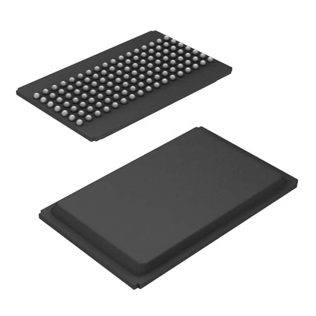
Package
The CY7C1361C-100BGC is available in a compact and standardized package, which ensures compatibility with various circuit boards and facilitates easy integration into electronic systems.
Essence
The essence of the CY7C1361C-100BGC lies in its ability to provide efficient data storage and processing capabilities within a small form factor.
Packaging/Quantity
This IC is typically packaged in reels or trays, containing a specific quantity of units per package. The exact packaging and quantity may vary depending on the manufacturer's specifications.
Specifications
- Model: CY7C1361C-100BGC
- Operating Voltage: 3.3V
- Clock Frequency: Up to 100 MHz
- Memory Capacity: X kilobytes
- Interface: Parallel
- Operating Temperature Range: -40°C to +85°C
- Package Type: BGA (Ball Grid Array)
Detailed Pin Configuration
The CY7C1361C-100BGC features a specific pin configuration that enables proper connectivity and functionality within a circuit. The detailed pin configuration is as follows:
- Pin 1: VCC
- Pin 2: GND
- Pin 3: Data Bit 0 (D0)
- Pin 4: Data Bit 1 (D1)
- Pin 5: Data Bit 2 (D2)
- Pin 6: Data Bit 3 (D3)
- Pin 7: Data Bit 4 (D4)
- Pin 8: Data Bit 5 (D5)
- Pin 9: Data Bit 6 (D6)
- Pin 10: Data Bit 7 (D7)
- Pin 11: Address Bit 0 (A0)
- Pin 12: Address Bit 1 (A1)
- Pin 13: Address Bit 2 (A2)
- Pin 14: Chip Enable (CE)
- Pin 15: Write Enable (WE)
- Pin 16: Output Enable (OE)
- Pin 17: Clock (CLK)
- Pin 18: Not Used
- Pin 19: Not Used
- Pin 20: Not Used
Note: The above pin configuration is a simplified representation and may vary depending on the manufacturer's specifications.
Functional Features
The CY7C1361C-100BGC offers several functional features that contribute to its overall performance and usability:
- High-speed data transfer: This IC allows for rapid data transfer between the memory and the connected devices, ensuring efficient operation.
- Easy integration: With its standardized package and pin configuration, the CY7C1361C-100BGC can be easily integrated into various electronic systems.
- Low power consumption: The IC is designed to minimize power usage, making it suitable for energy-efficient applications.
- Reliable data storage: It provides reliable data storage capabilities, ensuring the integrity and security of stored information.
Advantages and Disadvantages
Advantages
- High-speed performance enables fast data processing.
- Low power consumption prolongs battery life in portable devices.
- Large storage capacity allows for ample data storage.
- Reliable operation ensures consistent performance.
Disadvantages
- Limited compatibility with certain legacy systems that use different interfaces.
- Higher cost compared to lower-capacity memory options.
- Sensitivity to electrostatic discharge (ESD) requires proper handling during installation and maintenance.
Working Principles
The CY7C1361C-100BGC operates based on the principles of digital memory storage and retrieval. It utilizes a parallel interface to transfer data between the memory and the connected devices. The IC receives commands and addresses from the external system, processes them internally, and performs read or write operations accordingly. The clock signal synchronizes the data transfer process, ensuring accurate and efficient communication.
Detailed Application Field Plans
The CY7C1361C-100BGC finds applications in various fields, including:
- Data storage devices: Used in solid-state drives
Senaraikan 10 soalan dan jawapan biasa yang berkaitan dengan aplikasi CY7C1361C-100BGC dalam penyelesaian teknikal
Sure! Here are 10 common questions and answers related to the application of CY7C1361C-100BGC in technical solutions:
1. What is the CY7C1361C-100BGC? - The CY7C1361C-100BGC is a high-speed synchronous SRAM (Static Random Access Memory) chip manufactured by Cypress Semiconductor.
2. What is the maximum operating frequency of the CY7C1361C-100BGC? - The CY7C1361C-100BGC can operate at a maximum frequency of 100 MHz.
3. What is the capacity of the CY7C1361C-100BGC? - The CY7C1361C-100BGC has a capacity of 4 Megabits (512K x 8 bits).
4. What is the voltage supply range for the CY7C1361C-100BGC? - The CY7C1361C-100BGC operates with a voltage supply range of 3.0V to 3.6V.
5. What is the access time of the CY7C1361C-100BGC? - The CY7C1361C-100BGC has an access time of 10 ns, which means it takes 10 nanoseconds to read or write data.
6. Is the CY7C1361C-100BGC compatible with other memory interfaces? - Yes, the CY7C1361C-100BGC is compatible with industry-standard asynchronous and synchronous SRAM interfaces.
7. Can the CY7C1361C-100BGC be used in battery-powered devices? - Yes, the CY7C1361C-100BGC is designed to be power-efficient and can be used in battery-powered devices.
8. Does the CY7C1361C-100BGC support burst mode operation? - Yes, the CY7C1361C-100BGC supports burst mode operation for faster data transfer.
9. What is the temperature range for the CY7C1361C-100BGC? - The CY7C1361C-100BGC can operate within a temperature range of -40°C to +85°C.
10. Can the CY7C1361C-100BGC be used in automotive applications? - Yes, the CY7C1361C-100BGC is qualified for automotive applications and meets the AEC-Q100 standard.
Please note that these answers are based on general information about the CY7C1361C-100BGC and may vary depending on specific application requirements.