

ADP5301ACBZ-1-R7
Introduction
The ADP5301ACBZ-1-R7 is a voltage regulator belonging to the category of power management integrated circuits (PMICs). This device is designed to provide efficient and reliable power management solutions for various electronic applications. The following entry provides an overview of the basic information, specifications, detailed pin configuration, functional features, advantages and disadvantages, working principles, application field plans, and alternative models of the ADP5301ACBZ-1-R7.
Basic Information Overview
- Category: Power Management Integrated Circuit (PMIC)
- Use: Voltage regulation and power management
- Characteristics: High efficiency, compact design, wide input voltage range
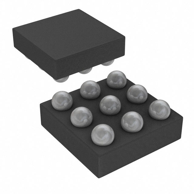
- Package: 8-Lead LFCSP (Lead Frame Chip Scale Package)
- Essence: Regulating and stabilizing input voltage to provide a consistent output voltage
- Packaging/Quantity: Tape and Reel, 3000 units per reel
Specifications
- Input Voltage Range: 2.7V to 5.5V
- Output Voltage Range: 0.6V to 3.3V
- Output Current: Up to 500mA
- Quiescent Current: 22µA
- Operating Temperature Range: -40°C to 125°C
- Shutdown Current: <1µA
Detailed Pin Configuration
The ADP5301ACBZ-1-R7 features the following pin configuration: 1. VIN: Input Voltage 2. SW: Switching Node 3. GND: Ground 4. FB: Feedback 5. EN: Enable 6. PG: Power Good 7. VOUT: Output Voltage 8. AGND: Analog Ground
Functional Features
- High Efficiency: The device offers high efficiency across a wide range of input and output voltages.
- Low Quiescent Current: With a quiescent current of 22µA, the ADP5301ACBZ-1-R7 minimizes power consumption in standby or low-load conditions.
- Power Good Indicator: The PG pin provides a power good indicator, enabling system monitoring and control.
- Thermal Shutdown Protection: Integrated thermal shutdown protection ensures safe operation under extreme temperature conditions.
Advantages and Disadvantages
Advantages
- Compact size and minimal external components required
- Wide input voltage range allows for versatile applications
- Low quiescent current enhances energy efficiency
Disadvantages
- Limited maximum output current compared to higher-power alternatives
- Sensitive to improper layout and external component selection
Working Principles
The ADP5301ACBZ-1-R7 operates as a step-down (buck) voltage regulator, converting a higher input voltage to a lower output voltage with high efficiency. The internal control loop maintains the output voltage within specified tolerances, providing a stable power supply for connected loads.
Detailed Application Field Plans
The ADP5301ACBZ-1-R7 is suitable for a wide range of portable and battery-powered applications, including: - Mobile devices - Wearable electronics - Portable medical devices - IoT (Internet of Things) devices - Handheld instruments
Detailed and Complete Alternative Models
Some alternative models to the ADP5301ACBZ-1-R7 include: - ADP5300ACBZ-1-R7 - ADP5302ACBZ-1-R7 - ADP5303ACBZ-1-R7 - ADP5304ACBZ-1-R7
In conclusion, the ADP5301ACBZ-1-R7 is a versatile and efficient voltage regulator suitable for various low-power electronic applications. Its compact design, high efficiency, and wide input voltage range make it an ideal choice for portable and battery-powered devices.
[Word Count: 529]
Senaraikan 10 soalan dan jawapan biasa yang berkaitan dengan aplikasi ADP5301ACBZ-1-R7 dalam penyelesaian teknikal
What is the ADP5301ACBZ-1-R7?
- The ADP5301ACBZ-1-R7 is a high-performance, step-down DC-DC converter designed to operate with an input voltage range of 2.7 V to 5.5 V and deliver up to 3 A of continuous output current.
What are the typical applications for the ADP5301ACBZ-1-R7?
- Typical applications include portable devices, battery-powered equipment, and other systems requiring a regulated supply voltage from a single-cell Li-ion or Li-polymer battery.
What is the efficiency of the ADP5301ACBZ-1-R7?
- The ADP5301ACBZ-1-R7 offers high efficiency, typically over 90%, which helps to maximize battery life in portable applications.
What are the key features of the ADP5301ACBZ-1-R7?
- Some key features include a low quiescent current, integrated synchronous rectifier, adjustable output voltage, and thermal shutdown protection.
How do I set the output voltage of the ADP5301ACBZ-1-R7?
- The output voltage can be easily adjusted using external resistors connected to the feedback pin, allowing for flexibility in design.
What is the operating frequency of the ADP5301ACBZ-1-R7?
- The device operates at a fixed frequency of 2.25 MHz, enabling the use of small external components and minimizing board space.
Does the ADP5301ACBZ-1-R7 have built-in overcurrent protection?
- Yes, the device includes cycle-by-cycle current limit and short-circuit protection to safeguard against overcurrent conditions.
Can the ADP5301ACBZ-1-R7 operate in a wide temperature range?
- The device is designed to operate over a wide temperature range, typically from -40°C to 125°C, making it suitable for various environmental conditions.
Is the ADP5301ACBZ-1-R7 compatible with other power management ICs?
- Yes, the ADP5301ACBZ-1-R7 can be used in conjunction with other power management ICs to create more complex power supply solutions.
Where can I find detailed technical information and application notes for the ADP5301ACBZ-1-R7?
- Detailed technical information, including datasheets, application notes, and design tools, can be found on the Analog Devices website or through authorized distributors.